Get Started

creative tool

Process Functional Modeling

intro image

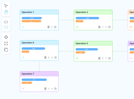
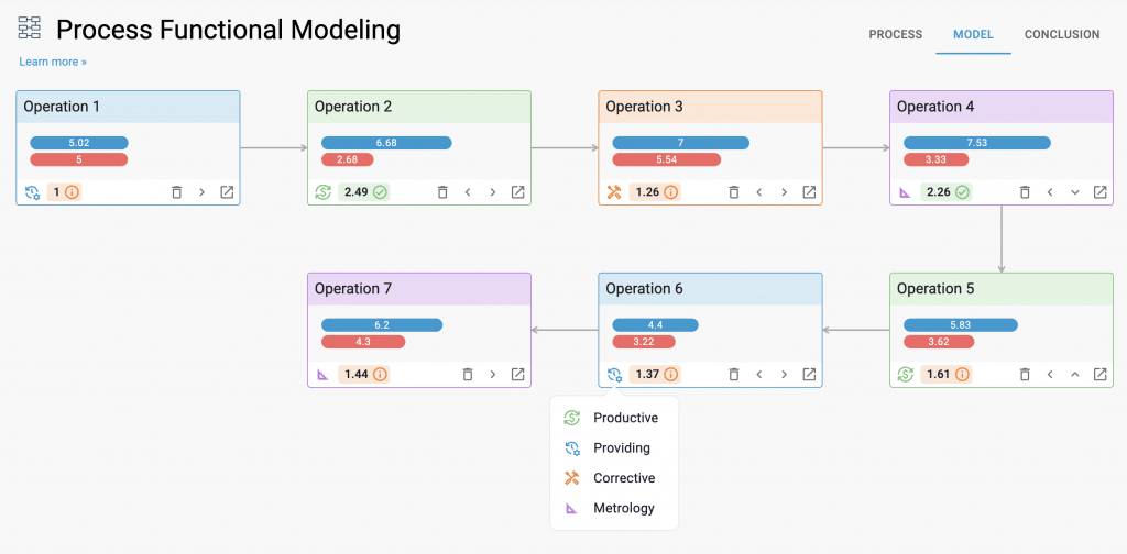
Process Functional Modeling (PFM) is an analytical tool to learn the process through modeling of different operations, solving problems, and defining ways to the improvement of any fabrication process. PFM is an extension of the System Functional Modeling (SFM) and it allows us to analyze the whole process vs one particular operation in the process.
What will you get from the Process Functional Modeling?

  • Learn and understand how a process operates
  • Visualize and understand each operation within a process
  • Analyze and comprehend the functional value and contribution of each operation within a process
  • Make strategic and tactical decisions for process improvements
  • Create a common language within the organization

When should you use Process Functional Modeling?

Among many cases when Process Functional Modeling is useful for us as problem solvers and innovators, we want to highlight just a few:

  • Process design
  • Improve existing processes
  • Reduce the complexity of a process and reduce costs
  • Improve process yield
  • Identify redundant and low-value operations
  • Lean, Kaizen, and similar events

Benefits of Implementing Process Functional Modeling

Implementing PFM can lead to significant improvements in operational efficiency. By breaking down each operation within a process, organizations can pinpoint specific areas that require enhancement. This detailed understanding helps in reducing bottlenecks, improving throughput, and ultimately increasing overall productivity. Additionally, PFM facilitates better communication among team members as it establishes a clear and common understanding of the process, ensuring everyone is aligned with the goals and objectives.

Future Trends in Process Functional Modeling

As technology continues to evolve, the integration of advanced tools such as artificial intelligence and machine learning with PFM is becoming more prevalent. These technologies can enhance the analytical capabilities of PFM, allowing for real-time monitoring and more accurate predictions of process performance. Additionally, the increasing adoption of digital twins—a virtual replica of physical processes—enables organizations to simulate and test process changes in a risk-free environment before implementing them in the real world. These trends are set to further revolutionize the way businesses optimize their processes.

Join 1000+ users today

Speedup your innovation

Start for free now

Showcasing Successful Projects

Microelectronics

Wafer cleaning issues at the wet process

Wet cleaning is widely used in microchip manufacturing. Single wafer equipment is working as follows. A wafer rotates, and chemistry is poured from a movable nozzle. Water rinsing is performed at the end of the process. Loading of a new batch of the chemistry resulted in excursion - a strongly increased amount of defects was observed on the wafer after the processing. The project is dedicated to the failure analysis and creation of innovative solutions.

user avatar
Dr. Anatoly Agulyansky
Microelectronics

Optimizing IC Interconnection: A Functional Approach to Innovation (Stay updated on the project's progress)

Semiconductor devices are becoming more complex and expensive. But what exactly are we paying for when we buy a computer, cellphone, or any device containing a microchip? It’s not for radically new functions—the core components remain the same: transistors and interconnections. According to Moore’s law, transistors are getting smaller, with more interconnection layers added, making the manufacturing process longer and more costly.In reality, we’re paying for the inability of engineers to efficiently solve engineering challenges.This project leverages System Functional Modeling (SFM) to analyze the IC interconnection layer and Process Functional Modeling (PFM) to evaluate its manufacturing process. These analyses aim to deepen our understanding of both the device and the production process, generating innovative solutions for cost reduction and improved efficiency.

user avatar
Dr Anatoly Agulyansky
Microelectronics

SiO2 thin film creation in Diffusion furnace - Process Functional Modeling

The process is related to microelectronics - microchip manufacturing.The purpose of the process is to create a SiO2 layer on the surface of a Si wafer. Equipment: Vertical furnace to heat the wafers in the Q2 atmosphere and perform oxidation on the wafer surface. Process: The oxidation occurs on the front side and on the back side of the wafer Requirements: Create a SiO2 thin layer with a certain thickness and low sigma - low standard deviation of the thickness between the wafers and within the waferFailure: Wafers from the lower zone have higher thickness and significantly higher within wafer sigma (standard deviation of the thickness within the wafer)

user avatar
Dr. Anatoly Agulyansky
Environment

Targets splinters after trapshooting contaminate the nature - how to solve this problem

A good example of how to use 40 Inventive Principles for ideas generation.

user avatar
Dr. Anatoly Agulyansky
Mechanics

Functional Modeling of a Vacuum Cleaner: A Pathway to Innovation

This project showcases how functional modeling can drive innovation by analyzing and simulating various versions of a vacuum cleaner. By studying the functional model, you will experience firsthand how the Functional Modeling creative thinking tool helps identify opportunities for improvement and generate innovative ideas for the next generation of products.Through this example, you’ll learn how to dissect the functionality of a vacuum cleaner, revealing ways to enhance its performance, efficiency, and user experience—ultimately paving the way for future innovations.

user avatar
Dr. Anatoly Agulyansky
Microelectronics

Wafer breakage at flash heating

Flash heating of a wafer is widely used in microchip manufacturing. The purpose of the process is to prevent the diffusion of ions and atoms. During the flash process, a wafer breakage occurs. The project's purpose is to learn and understand the mechanism of the wafer breakage and propose the solutions to prevent the wafer breakage

user avatar
Dr. Anatoly Agulyansky
Chemistry

מניעת עיבוי על העדשות - רוני עוז ותומר קליין

?כיצד נוכל למנוע הצטברות של אדים על גבי העדשה בתנאי סביבה שונים כדי לשפר את הראייה והבטיחות

user avatar
Roni Oz
Environment

Recycling waste of solar panels.students: Alaa & saed

Excited to share our latest project at Ben-Gurion University of the Negev! 🚀 We tackled the pressing issue of solar panel waste and explored innovative recycling solutions to make solar energy truly sustainable.Key insights:Solar panel waste could hit 78 million metric tons by 2050. Only 10% of panels are currently recycled in the EU. Our project highlights the need for efficient recycling technologies, better regulations, and economic incentives to drive sustainable practices.Let’s work together for a greener future! 🌱

user avatar
Saed Hasson