Get Started Free

Engineering Problem Solving Software

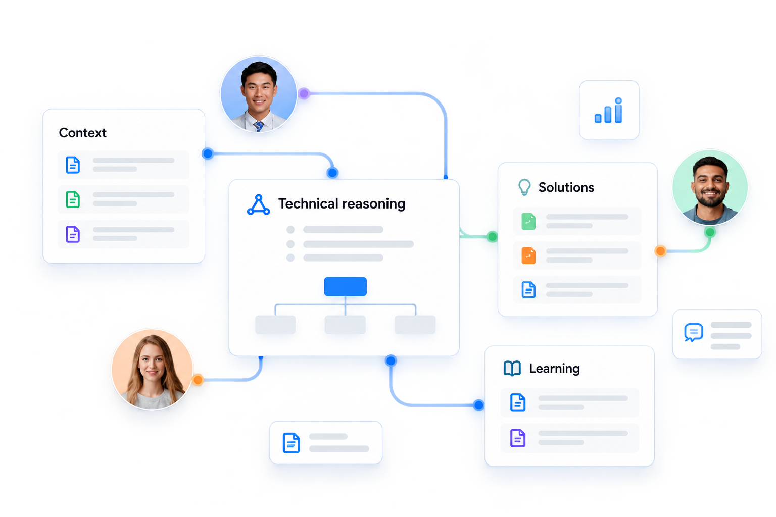
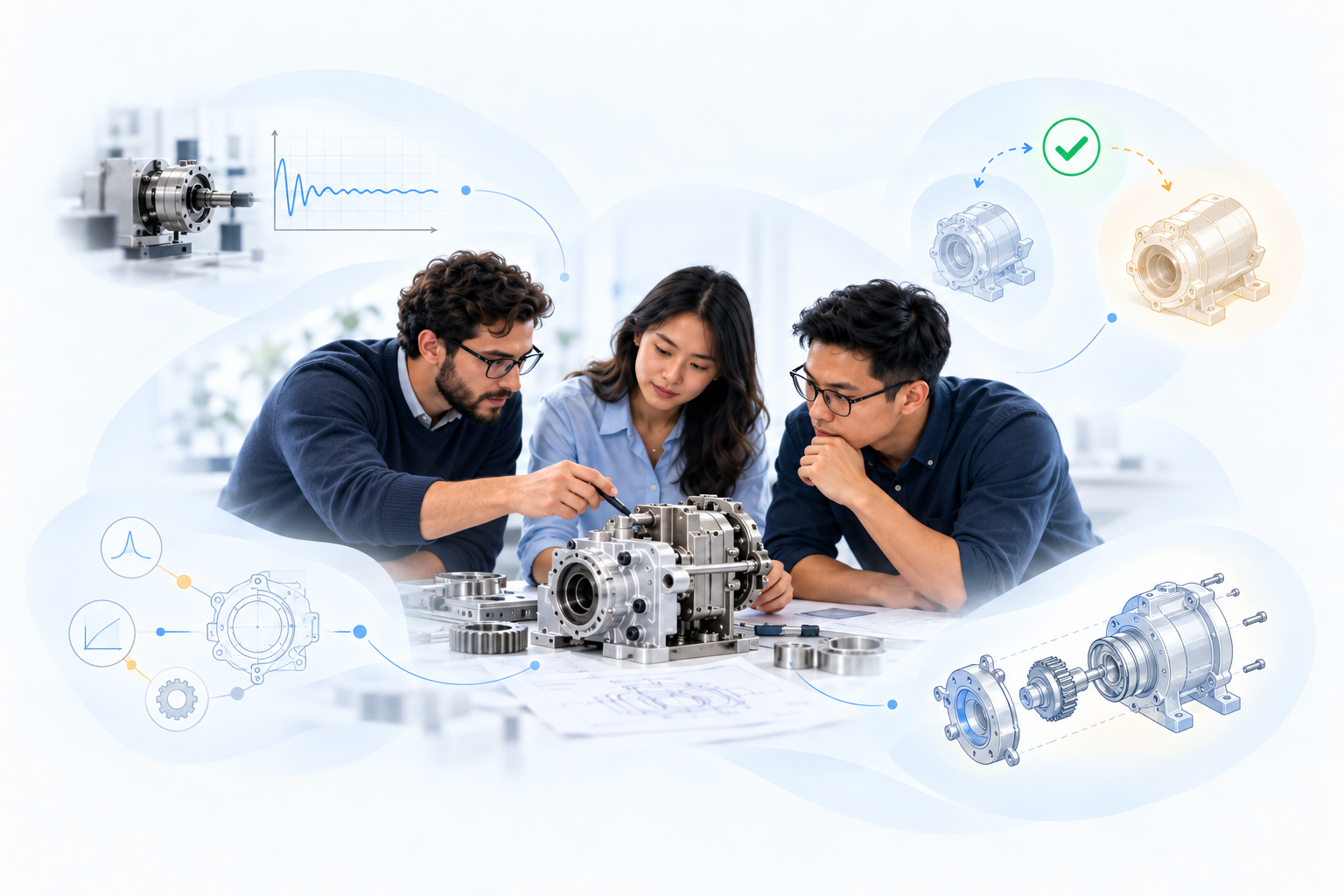
PRIZ helps engineering teams model complex problems, understand failure mechanisms, and systematically develop innovative solutions that improve yield, quality, and manufacturing cost.

VP Engineering photo
PRIZ gave our team a structured way to move from firefighting to real root-cause thinking. It helped us align faster and turn investigations into reusable learning.
VP Engineering · Semiconductor manufacturer
Faster alignment Less firefighting Reusable knowledge

TRUSTED BY TOP COMPANIES

company logo
company logo
company logo
company logo
company logo
company logo
company logo
company logo
company logo
company logo
company logo
company logo
company logo
company logo
company logo
company logo
company logo
company logo
company logo
company logo
company logo
company logo
company logo
company logo
company logo
company logo
company logo
company logo
company logo
company logo

Turn engineering pain into your repeatable wins

PRIZ Guru gives you a guided, no-guesswork workflow for root cause analysis, process improvement, and systematic innovation, so you spend less time firefighting and more shipping reliable, profitable outcomes.

Incidents Chronic problems High cost Low yield Culture of systematic innovation

Faster containment. Stronger fixes. Fewer repeats.

  • Move from chaos to clarity fast
  • Get to root cause with evidence
  • Prevent recurrence by default
Request a Demo
Process Engineering Lead • Semiconductor manufacturer
PRIZ helped us stop jumping to fixes and first understand what was really happening.
Process Engineering Lead · Semiconductors
image

Make “unsolvable” problems solvable again.

  • Expose why the problem persists
  • Reveal what blocks solutions
  • Turn every solved issue into a reusable asset
Request a Demo
Continuous Improvement Manager • Advanced manufacturing
The value was not just solving one issue. It was finally seeing why the problem kept coming back.
Continuous Improvement Manager · Advanced manufacturing
image

See where the money goes. Then control it.

  • Trace cost back to process mechanisms
  • Reduce cost without sacrificing performance
  • Make cost reduction part of your operating system
Request a Demo
Operations Director • Semiconductor manufacturer
The discussion shifted from opinions to mechanisms, actions, and measurable business impact.
Operations Director · Semiconductor manufacturer
image

Diagnose yield loss mechanisms. Improve yield predictably.

  • Identify the mechanism behind yield loss
  • Run better experiments
  • Build a yield-improvement habit
Request a Demo
Yield Engineering Manager • Fab
PRIZ gave the team a disciplined way to connect symptoms, process conditions, and root-cause hypotheses.
Yield Engineering Manager · Fab
image

One language. Less politics. More compounding learning.

  • A shared engineering language
  • Collaboration that complements
  • From “event-driven improvement” to a predictable pulse
Request a Demo
Engineering Excellence Lead • Global manufacturing
It gave engineers a shared language. The meetings became clearer, faster, and less political.
Engineering Excellence Lead · Manufacturing
image

Elevate problem-solving with tools and methods

PRIZ Guru is a methodology-first innovation platform that systematizes problem solving and helps teams generate the innovative solutions companies need to stay competitive and profitable. With a unified toolkit of structured methods and processes, PRIZ strengthens engineering thinking and promoting seamless communication among all stakeholders.

Creative thinking tools Guided Facilitation (AI Optional) Project management Collaboration Automatic reporting Idea management

Creative thinking tools

Our platform offers a range of creative thinking tools that help you think outside the box and develop new, innovative solutions.

Learn more
feature image

Guided Facilitation (AI Optional)

Guided facilitation walks teams through a structured, repeatable process that strengthens engineering thinking, drives continuous improvement, and embeds consistent learning across the organization. Works fully without AI; an optional assistant can speed feedback, research, and reporting.

Learn more
feature image

Project management

Our platform offers a seamless integration between project management and your problem-solving process.

Learn more
feature image

Collaboration

Our platform promotes open communication, shared goals, conflict resolution, collective ownership, trust, and positive relationships among all stakeholders.

Learn more
feature image

Automatic reporting

Engineers no longer have to do the most boring part of problem-solving - writing a report for stakeholders - as the report is automatically generated for them.

Learn more
feature image

Idea management

The ultimate goal of every project is to generate innovative ideas and solutions. PRIZ Platform's idea management provides full transparency of all ideas and decisions made throughout a project.

Learn more
feature image

Showcasing Successful Projects

Microelectronics

Radial CDO Non-Uniformity Causing Wafer Edge Speed Loss

This project investigates radial non-uniformity of CDO low-k dielectric deposited by PECVD and its possible impact on wafer performance. Final test data indicate that faster dies are mainly located closer to the wafer center, while slower dies are more often found near the wafer periphery. The corresponding RC-delay trend also increases toward the wafer edge. The focus of the project is the capacitance component of RC-delay. CDO is expected to provide a low dielectric constant between BEOL metal lines, but the deposited film may not have uniform properties across the wafer. Near the wafer edge, the process can be influenced by different gas flow, plasma behavior, residence time, temperature, and pumping conditions. This may lead to stronger oxidation and deeper precursor decomposition near the periphery, forming CDO that is more oxygen-rich, less carbon-rich, denser, and closer in behavior to SiO₂. As a result, the dielectric constant k may increase toward the wafer edge, causing higher interline capacitance, higher RC-delay, and lower die speed. The project uses Functional Modeling to understand how PECVD chamber components and process conditions affect CDO film properties. The goal is to identify the main functional and problematic interactions and propose directions for compensation, such as radial gas-flow tuning, multi-zone showerhead design, edge compensation flow, and local plasma or temperature control.

user avatar
Dr Anatoly Agulyansky
Microelectronics

Wafer cleaning issues at the wet process

Wet cleaning is widely used in microchip manufacturing. Single wafer equipment is working as follows. A wafer rotates, and chemistry is poured from a movable nozzle. Water rinsing is performed at the end of the process. Loading of a new batch of the chemistry resulted in excursion - a strongly increased amount of defects was observed on the wafer after the processing. The project is dedicated to the failure analysis and creation of innovative solutions.

user avatar
Dr. Anatoly Agulyansky
Microelectronics

Ta PVD Target Racetrack Erosion Reduces Target Utilization - Functional Modeling

This project investigates the nonuniform erosion of an expensive Ta sputtering target during Ta/TaN PVD. A deep racetrack groove forces target replacement while a significant amount of tantalum remains unused. Using PRIZ problem-solving tools, the project explores the system’s functions, identifies the root causes of localized erosion, and develops ways to improve target utilization without reducing deposition rate or production throughput.

user avatar
Dr Anatoly Agulyansky
Microelectronics

SiO2 thin film creation in Diffusion furnace - Process Functional Modeling

The process is related to microelectronics - microchip manufacturing. The purpose of the process is to create a SiO2 layer on the surface of a Si wafer. Equipment: Vertical furnace to heat the wafers in the Q2 atmosphere and perform oxidation on the wafer surface. Process: The oxidation occurs on the front side and on the back side of the wafer Requirements: Create a SiO2 thin layer with a certain thickness and low sigma - low standard deviation of the thickness between the wafers and within the wafer Failure: Wafers from the lower zone have higher thickness and significantly higher within wafer sigma (standard deviation of the thickness within the wafer)

user avatar
Dr. Anatoly Agulyansky

Our courses

We offer a variety of courses to help you learn how to use our app to solve problems. Our courses are designed for users of all skill levels, from beginners to experienced users. Our courses include video lessons, hands-on exercises, and support from experienced instructors.